

Events
News
19 Mar, 2024
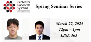
CNS Spring Seminar Series
Semiconductor Bio-interface for DNA Data Storage Dr. Woo-Bin Jung, Harvard University
Semiconductor Bio-Interface for Functional Synaptic Connection Mapping Dr. Jung Wang, Harvard University
March 22, 2024 | 12pm – 1pm | LISE 303
About Speakers: Dr. Woo-Bin Jung and Dr. Jun Wang are postdoctoral fellows in Prof. Donhee Ham’s Lab, Harvard University.
[+MORE]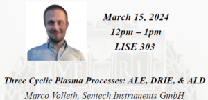
13 Mar, 2024
Special CNS Seminar: Three Cyclic Plasma Processes: ALE, DRIE, & ALD
Marco Volleth, Sentech Instruments GmbH
March 15, 2024 | 12pm – 1pm | LISE 303
Abstract: For some time now, plasma processes have not only been carried out
continuously, but also used in a cyclical manner. The best-known process of this type is the
so-called Bosch process for deep etching of silicon (DRIE). There is also atomic layer
deposition (ALD) for depositing very thin layers with high precision and conformality. The
equivalent etching process, called atomic layer etching (ALE), is used in more and more
applications. In the lecture, these three cyclic plasma processes will be examined in more
detail and applications will be shown using examples from SENTECH customers and our
application lab.
About Speaker: Marco Volleth studied nanotechnology with a bachelor's degree at the
Friedrich-Alexander University of Erlangen from 2013 until 2017, followed by a master's
degree in Electrical and Microsystems Engineering at the University of Applied Sciences in
Regensburg (both Germany). The main focus of his studies was in the areas of lithography
and reactive ion etching, especially for the two-material systems silicon and gallium nitride.
Since October 2020 he is working as an Application Engineer for plasma etching at
SENTECH Instruments in Berlin, Germany. SENTECH is a manufacturer of plasma process
systems and devices for thin-film metrology.
Recent Publications
-
A new metamaterial for MRI-safe deep brain stimulation leads
10.1109/ICEAA57318.2023.10297949
-
Scanning multiprobe microscopy for mesoscopic devices and materials: Part II
Bulletin of the American Physical Society, 2024
-
Scanning multiprobe microscopy for mesoscopic devices and materials: Part I
Bulletin of the American Physical Society, 2024
-
Reconfigurable photonic integrated circuits based on liquid-crystal-cladded slab waveguides
https://spie.org/photonics-west/presentation/Reconfigurable-photonic-integrated-circuits-based-on-liquid-crystal-cladded-slab/12890-52
-
Observation of Electronic Viscous Dissipation in Graphene Magneto-thermal Transport
APS March Meeting 2024, Abstract: M07.00008
-
Ecological and phylogenetic signals in catarrhine root morphology
Conference presentation, American Association of Biological Anthropologists
-
Time-stepped optical frequency comb laser design leveraging three-dimensional integration of thin-film lithium niobate and silicon CMOS
https://spie.org/photonics-west/presentation/Time-stepped-optical-frequency-comb-laser-design-leveraging-three-dimensional/12890-34
-
Compact and wideband nanoacoustic pass-band filters for future 5G and 6G cellular radios
Giribaldi, G., Colombo, L., Simeoni, P. et al. Compact and wideband nanoacoustic pass-band filters for future 5G and 6G cellular radios. Nat Commun 15, 304 (2024). https://doi.org/10.1038/s41467-023-44038-9
-
Staphylococcus aureus AbcA transporter enhances persister formation under β-lactam exposure
Truong-Bolduc et al., “Staphylococcus Aureus AbcA Transporter Enhances Persister Formation under β-Lactam Exposure.”
-
Fractional quantum anomalous Hall effect in multilayer graphene
Lu, Z., Han, T., Yao, Y. et al. Fractional quantum anomalous Hall effect in multilayer graphene. Nature 626, 759–764 (2024). https://doi.org/10.1038/s41586-023-07010-7
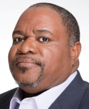 WILLIAM WILSON
EXECUTIVE DIRECTOR
Directors Welcome
The Center for Nanoscale Systems (CNS) at Harvard University was created with a very clear vision: To provide a collaborative multi-disciplinary research environment to support of the creation and evolution of world-class nanoscience and technical expertise, for the Harvard research community as well as the larger community of external researchers both from academia and industry.
Our Core Values:
Facilitating leading-edge, multi-disciplinary, research a
[+MORE] ROBERT WESTERVELT
DIRECTOR