

Open Positions
Information on open positions will be posted here when available
Current Open CNS Positions:
Principal Optical Scientist
- Cambridge, Massachusetts, United States
- Full-time
- Work Format: Fully On-Site
- Harvard Job Function: Research
- Union: 65 – Harvard Academic Workers
- Salary Grade: 059
- Department: Sciences – Center for Nanoscale Systems
- FLSA Status: Exempt
Job Summary:
Oversee and execute a range of complex scientific research in a core facility environment including planning and optimizing research, designing analysis algorithms, and providing training to researchers, faculty, and staff.
Job-Specific Responsibilities:
The Center for Nanoscale Systems (CNS) at Harvard University seeks enthusiastic individual to work within the Imaging and Analysis Group as a Senior Scientist devoted to our Optical Spectroscopy Core.
The position will train and support users in the use of a wide variety of standard spectral techniques, UV/Vis. FTIR, Raman, etc. In addition, the role will support the development and training of a range of next generation spectral tools including, Nonlinear Optical Imaging, Scan Probe Optical Imaging and Spectroscopic Techniques, as well as Ultrafast Optics support. CNS is an open, shared-use facility that serves all of Harvard as well as external academic and industrial users.
Working under the supervision of the CNS Executive Director and the Imaging and Analysis Facility Manager, this person will oversee the rapidly evolving and expanding spectroscopy laboratory.
Helping users in fields ranging from Chemistry, Biology, Physics, and Engineering. The goal will be to support exciting, emerging, new areas of research and CNS expects to be at the cutting edge of these technologies.
The incumbent must be extremely well versed in linear and nonlinear optics, nanooptics, and nanophotonics, and have a detailed understanding of the design, construction, and development of optical systems. These tools are defining an entirely new realm of nanoscale materials and device characterization, and they will become essential tools in the advancement of world-class nanoscience. To this end this person will serve as one of the focal points of Optical technology advancement for CNS. As such, the applicant must be comfortable with instrument development, training new facility users on sample preparation, instrument operation, and computational data analysis.
The candidate needs to have advanced knowledge and experience in operation of an array of imaging paradigms for optical characterization.
In addition, the incumbent must be familiar with ultrafast laser based spectral imaging systems, particularly in the area of ultra-high-resolution optical imaging.
The incumbent will become resource for collaboration and must have strong written and verbal communication skills.
The candidate will also perform work for remote CNS users. Detailed record keeping of instrument activity, experimental results, maintenance and repair logs, and operating procedures is expected.
Working Conditions:
- May be exposed to bloodborne pathogens, primary tissue, cell lines or infectious materials
- May work in a research environment where animals are present
- May be exposed to toxic, radioactive, or carcinogenic materials including compressed gases, acids, solvents, vacuum pump oils, and other chemicals
- May be required to work nights and weekends
Physical Requirements:
Must be able to work in an imaging facility, cleanroom, biological, chemical, and measurement laboratory environments. Will work around compressed gases, acids, bases, oxidizers, solvents, vacuum pump oils, and other chemicals. Must be very dexterous; may be required to work on large and small assemblies.
Basic Qualifications:
PhD in in a related scientific discipline. Minimum of eight years’ relevant work experience
Additional Qualifications and Skills:
- Ph.D. in biology, chemistry, physics, engineering, or equivalent field. The candidate should have 3 or more years of nonlinear optical microscopy experience. Experience with image processing and analysis as well as basic understanding of computer scripting and instrument software development is required.
- The candidate must have significant experience in laboratory environments and be fully comfortable working in a spectroscopic imaging facility. The candidate needs to have advanced knowledge and experience in development and operation of Optical and Scan-probe instrumentation.
- The candidate should be self-motivated with a strong desire to acquire on-the-job training, to succeed, and to develop intellectual and practical professional skills. Excellent English and written skills required. Demonstrated ability to work well in teams and with graduate and undergraduate students is essential.
- 10+ years of experience and an Advanced degree in Materials Science, Physics, Applied Physics, Chemistry, Chemical Engineering, or related field is preferred. The candidate should have significant experience with optics and nanophotonics, both instrumentation and modeling, including the use of COMSOL multi-physics or other e-field modeling platforms. A demonstrated track record of research excellence and leadership in the Nonlinear Optical Imaging, Photonics and/or Scan-probe microscopy is expected. The individual would be expected to reach out to the vibrant local academic and industrial research base to raise the profile and expand the user base and application space for nanospectroscopy at Harvard CNS. Excellent reporting and communications skills are a must.
- Standard Hours/Schedule: 35 hours per week
- Visa Sponsorship Information: Harvard University is unable to provide visa sponsorship for this position
- Pre-Employment Screening: Identity, Education
- Other Information:
- All formal offers will be made by FAS Human Resources
- Work Format Details
This position has been determined by school or unit leaders that all duties and responsibilities must be performed at a Harvard or Harvard-designated location. Certain visa types may limit work location. Individuals must meet work location sponsorship requirements prior to employment.
Salary Grade and Ranges
This position is salary grade level 059. Please visit Harvard’s Salary Ranges to view the corresponding salary range and related information.
Benefits
Harvard offers a comprehensive benefits package that is designed to support a healthy work-life balance and your physical, mental and financial wellbeing. Because here, you are what matters. Our benefits include, but are not limited to:
- Generous paid time off including parental leave
- Medical, dental, and vision health insurance coverage starting on day one
- Retirement plans with university contributions
- Wellbeing and mental health resources
- Support for families and caregivers
- Professional development opportunities including tuition assistance and reimbursement
- Commuter benefits, discounts and campus perks
Learn more about these and additional benefits on our Benefits & Wellbeing Page.
EEO/Non-Discrimination Commitment Statement
Harvard University is committed to equal opportunity and non-discrimination. We seek talent from all parts of society and the world, and we strive to ensure everyone at Harvard thrives. Our differences help our community advance Harvard’s academic purposes.
Harvard has an equal employment opportunity policy that outlines our commitment to prohibiting discrimination on the basis of race, ethnicity, color, national origin, sex, sexual orientation, gender identity, veteran status, religion, disability, or any other characteristic protected by law or identified in the university’s non-discrimination policy. Harvard’s equal employment opportunity policy and non-discrimination policy help all community members participate fully in work and campus life free from harassment and discrimination.
Positions outside of CNS:
Metalenz: https://metalenz.com/career/fabrication-and-process-engineer/
Heat2Power, Inc.: Device Engineer
Heat2Power, Inc.: Process Technician
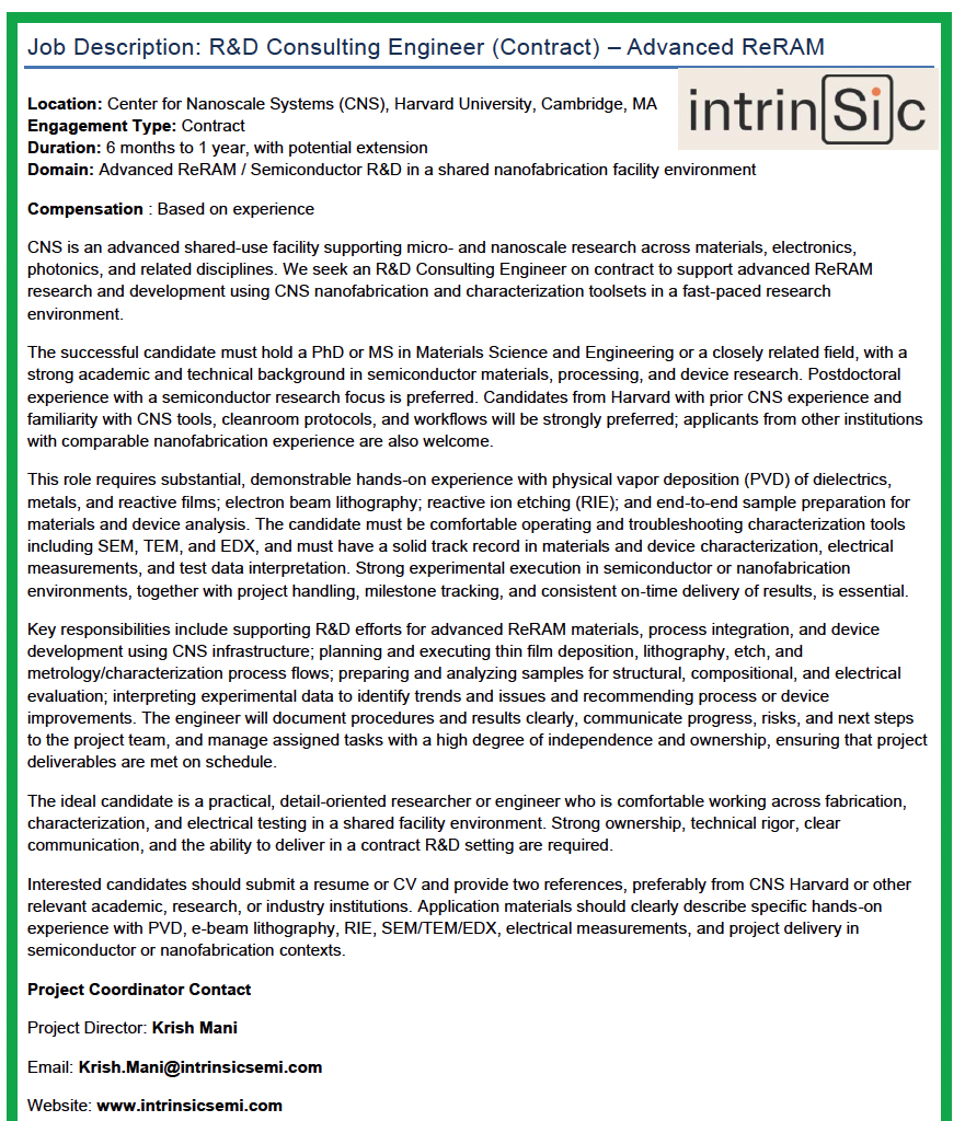
Intrinsic Semiconductor Technologies: R&D Consulting Engineer (Contract) – Advance ReRAM
for more information please see here
Applied Materials 2025 – 26 Process Engineer Co-op-Doctorate (Gloucester, MA)
for more information please visit here
Process Engineer – III-V Semiconductor Device Fabrication at Pendar Technologies
For more information please visit here
Scientist, Photonics & Semiconductors at Pendar Technologies
For more information please visit here
Postdoctoral Position Nano-Optics Innovation through Metasurfaces and Light Structuring at CNST, Milan
For more information please visit here
PhD Position Tailoring Light–Matter Interactions via Structured Light at Politecnico di Milano
For more information please visit here
PhD Position Light–Matter Interaction at the Nanoscale in 2D Materials at Politecnico di Milano
For more information please visit here