

Nanofabrication
The Center for Nanoscale Systems' Nanofabrication Facility provides resource and staff support for fabricating and characterizing nanoscale devices and structures.
Fabrication
Nanofabrication and growth are carried out in a 10,500 sq ft cleanroom. The instruments available support an extensive range of fabrication and processing techniques, enabling a vast array of device structures from novel materials, ranging from NV center diamonds and other color center materials to TMDC atomic layer materials, III-V semiconductors, and biologically inspired systems. Our facilities offer plasma enhanced and low pressure CVD systems for thin film growth, as well as an extensive development of Atomic Layer Deposition (ALD) technologies. In addition, CNS teams have developed world-class expertise in engineered surfaces and super-hydrophobicity. To fabricate nanoscale structures and devices, CNS has excellent facilities for high-resolution e-beam and optical lithography, including four e-beam writers, as well as a versatile set of reactive ion etch (RIE) and other etching systems. For soft materials and biological and biomedical applications, CNS offers a Soft Lithography foundry that can make a wide variety of microfluidic and soft robotic structures.
2017-1-17 11.0.45-T-Cells
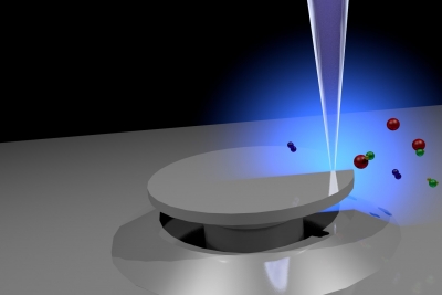
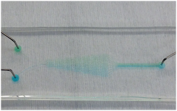
2017-1-17 11.0.45-0603Covercrop2
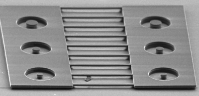
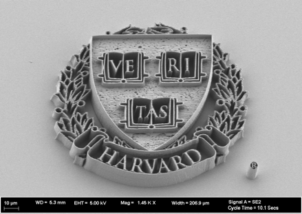
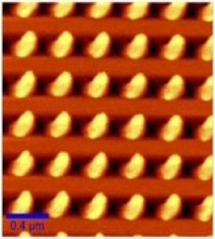
2017-1-17 11.0.45-nb_edited2
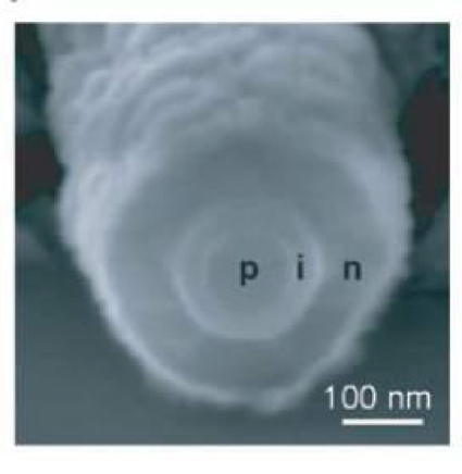
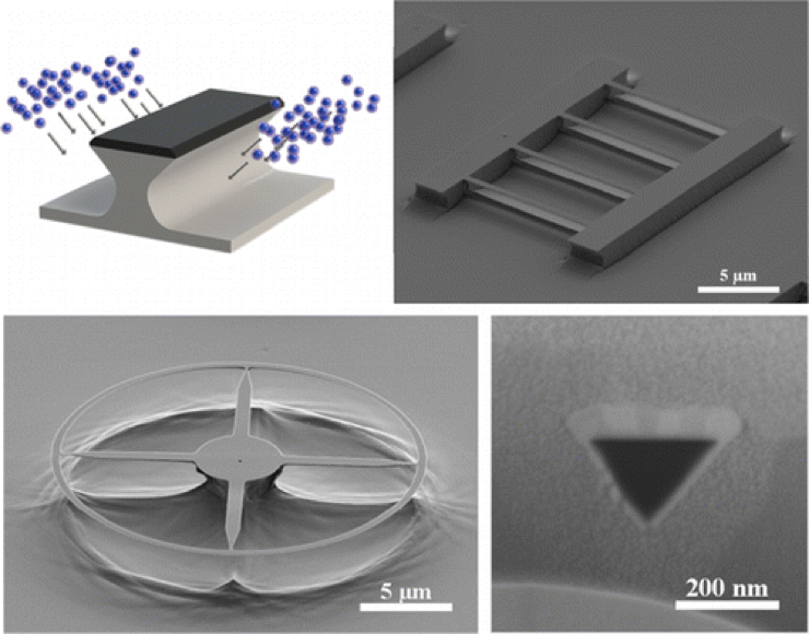
2017-1-17 11.0.45-disk4_0
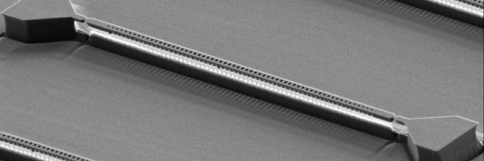
2017-1-17 11.0.45-nanobeam_cavity_0
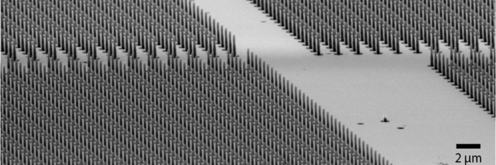
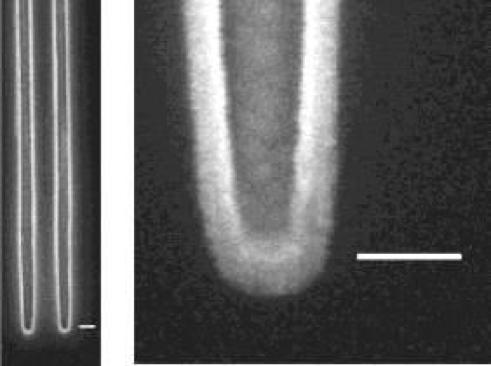
2017-1-17 11.0.45-diamondnanowires_0
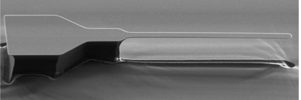
2017-1-17 11.0.45-diamond_cantilever_0
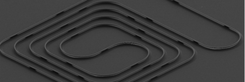
2017-1-17 11.0.45-angle_etched_ring_2
Lithography
Lithography is the core technology of any nanofabrication facility. The Center for Nanoscale Systems has established rigorous lithography solutions for a diverse variety of complex patterning requirements. These include highly advanced e-beam lithography systems for ultra-fine pattern writing, fast laser direct writing tools, a high throughput optical stepper, conventional mask aligners, and even a cutting edge 3D laser lithography system.
Photolithography
Photolithography is a fabrication process that uses light to transfer a geometric pattern from a photomask to a light sensitive material (photoresist) on the substrate. Photolithography is the cornerstone of modern IC manufacturing in current state of the art fabrication facilities. Optical photolithography capabilities at CNS include spinner benches for photoresist processing, multiple mask aligners, a stepper and multiple direct write systems capable of writing a photolithography pattern directly on the wafer and also capable of making a photography mask.
The recently acquired Nanoscribe 3D lithography system has added a new dimension to our photolithography capabilities. The Nanoscribe 3D lithography system has already proven itself to be an important system for research in areas including MEMS/NEMS, optics, photonics, microfluidics and many more.
More information on our Heidelberg DWL-66, Heidelberg uPG501, Heidelberg MLA150, Heidelberg MLA-2, Suss MA6, Suss MJB4, EVG 620 mask aligners, AS2000 in-line stepper, and our Nanoscribe 3D lithography system.
Electron-Beam Lithography EBL
Electron Beam Lithography (e-beam lithography or EBL) is an advanced lithography technology for creating ultrafine patterns (as small as 5nm) by using a focused electron beam. Derived from the scanning electron microscope, the technique in brief consists of scanning a beam of electrons in the desired pattern across a surface covered with an e-beam sensitive resist film.
CNS offers four advanced e-beam tools. Among them, the Elionix ELS-F125 system is the first EBL system in the world with 125KV acceleration voltage, which enables 5nm line width writing. Our knowledgeable staff has more than 20 years EBL experience across a large variety of applications.
More information on our Raith-150, JEOL JSM-7000F, Elionix ELS-7000, Elionix ELS-F125, and our Elionix HS50 e-beam lithography systems.
Thin Film Deposition
CNS offers two major semiconductor thin film deposition technologies for various nanofabrication processes, Chemical Vapor Deposition (CVD) and Physical Vapor Deposition (PVD). Chemical vapor deposition includes a group of film deposition equipment and processes whereby gaseous reactants can be deposited onto a substrate, such as LPCVD, PECVD, diamond PECVD, ALD, as well as several furnaces/ovens for film post processes. Our PVD capability at CNS includes thermal evaporators (TE), e-beam evaporators (EE), and sputtering deposition systems. More than 50 materials (dielectric, semiconductor, metal) are available in CNS’s thin film deposition facility. In addition, we have established a film process database, which provides users a deposition baseline recipe and film properties measurement data.
Chemical Vapor Deposition
At the Center for Nanoscale systems, we offer a variety of CVD techniques that can be utilized to create thin films for many different applications.
Three low pressure CVD systems (LPCVD) are available; a silicon nitride furnace, a polysilicon and amorphous silicon furnace as well as a TEOS furnace that grows silica (SiO2). We also have an atmospheric pressure CVD system (APCVD) that can oxidize silicon or other semiconductors to produce an oxide surface. All of the LPCVD and APCVD furnaces typically operate above 600C, but do provide the highest quality films in terms of purity, pinhole density, and conformality.
The CNS cleanroom also offers two plasma enhanced (PECVD) systems. The first system is based on standard parallel plate RF; this is used for growth of silica, silicon nitride and a:Si at temperatures from 190 to 300C, and dopant gases are available on this system. The second system uses a microwave and RF plasma to grow the same materials, but there are no dopant gases, the growth rates are much slower, however it produces high quality films at low temperatures (<150C). Finally we have a system for growing diamond films off of preexisting diamond surfaces using a hydrogen plasma and methane.
More information on our STS PECVD, Seiki Diamond Systems PECVD, and Oxford PlasmaPro 100 ICP-CVD systems.
Atomic Layer Deposition ALD
Atomic layer deposition (ALD) is a vacuum technology that allows the deposition of a wide variety of materials, at temperatures ranging from 300C down to room temperature. This technique makes use of alternating pulses of very reactive precursors to grow very thin (~1 Angstrom/cycle) layers of material on multiple substrates with extreme conformality and uniformity, as well as angstrom-level thickness control. Typical film thickness are between 1 nm to 100 nm. Higher thickness films can be deposited.
CNS offers a variety of ALD options, using thermal (non-plasma) ALD technology. Two 8” Savannah ALD systems (ALD-1 and ALD-4) from Cambridge Nanotech/Ultratech are available to deposit oxides, including Al2O3, HfO2, TiO2, ZnO, SiO2, and various nanolaminate combinations of these oxides. A third system, ALD-3, allows the use of ozone to grow a high quality SiO2, and metallic platinum at an unusually low temperature of 140C-150C. In addition, TiO2 and Al2O3 films are available on this unit. ALD-3 is set up to produce NiN and WiN films, which can be annealed down to relatively pure metallic films of Ni and W.
More information on our Savannah S200, Arradiance GEMStar, PdR-1, and Cambridge NanoTech S-200 ALD systems.
Physical Vapor Deposition
The Physical Vapor Deposition (PVD) area of the CNS Nanofabrication Facility consists of evaporators and sputter systems that can facilitate vacuum deposition of thin films utilizing over forty different materials, including conductive metals, semiconductors, and dielectrics. We have four thermal evaporators (TE) and two electron beam (e-beam) evaporation systems (EE) to accommodate depositions for lift-off processes with noble metals, magnetics, and more. These systems are cryo-pumped for reliability and designed to operate in the E-7 torr range.
We also have two sputter systems (SP) that are engineered for conformal deposition. This is good for insulators or flat films on featureless substrates. The sputter systems also have substrate heating for manipulation of the film crystal structure in-situ.
More information on our Key High, Sharon TE-3, Sharon TE-4 and Sharon TE-5 thermal evaporators, Sharon, Denton and PVD Products e-beam systems, AJA International 6-target and 3-target sputter systems, and PVD Products SEM sample sputtering system.
Etching
A wide range of wet and dry etching techniques are available in the CNS cleanroom to support the diverse fabrication portfolio of our users. Our dedicated wetbench set-ups support processes including several isotropic wet etching protocols and crystallographic orientation dependent Si KOH etching. Also available are a dry etching tools for controlled plasma etching and ion beam milling.
Dry Etching Processes
Dry etching is a key process for pattern transferring and surface treatment in micro/nano device fabrication. CNS has established strong dry etching capabilities for Si, III-V, diamond, oxide compound, metal, polymer and other materials. Users can select different advanced RIE technologies in CNS to meet their specific etching requirement, such as ICP, ECR, Bosch, NLD, XeF2, plasma ashing, and downstream ashing. Various etching recipes are available in the process database.
More information on our South Bay, Samco, Unaxis, STS, Anatech, Orbotech, Plasma-Therm, Matrix, Oxford, and Samco dry etching systems.
Wet Processing
CNS provides a range of wet processes for micro/nano fabrication, including lithography development, lift-off process, acid process, HF, TMAH, and critical point drying.
Metrology and Packaging
CNS has a large array of metrology instrument for measuring, monitoring, and characterizing every nanofabrication process, as well as device properties. Key metrology capabilities in nanofabrication include: electrical property characterization, optical property measurement, device CD monitoring, SPM techniques and advanced SEM. Packaging capability in CNS includes wafer dicing saw, wafer cleaver, flip-chip bonder and wire bonder.
Metrology
A large of array of measurement and characterization tools is available at CNS to provide traditional metrology and process control throughout the nanofabrication facilities. The contact surface profiler’s are commonly used for all-purpose step-height measurement of film thickness or etch depth. The scanning and spectroscopic ellipsometer’s are used regularly for film thickness uniformity and optical properties of transparent thin films. An optical profiler or white light interferometer is also available inside the cleanroom for surface topography, roughness, and step height measurements over large areas, while an AFM is also available to scan small areas of a wafer up to 6 inch diameter. The AFM has the highest lateral and vertical resolution for roughness, topography, and step heights with sub-nanometer resolution. There are several instruments supporting electrical characterization and device testing available including 4pt probe station with heated chuck as well as sheet resistance mapping for uniformity of PVD films or doping. A low-temperature, environmentally controlled 4pt probe station and Van der Pauw Hall system is also available. A Contact angle measurement system and critical-dimension SEM are offered inside the cleanroom in addition to many optical microscopes and digital cameras for quick inspection or measurements.
Soft Lithography Foundry, Nanotechnology, and Rapid Prototyping Lab
LISE G06 is a multi-functional space, acting as the soft lithography foundry, nanotechnology and rapid prototyping laboratory. Microfluidic devices can be assembled and tested in this space; an oxygen plasma etcher, UV flood exposure system, PDMS, and silane are supplied for G06 users. Additionally, a wax printer is provided for making paper-based microfluidic devices. For rapid prototyping purposes, two 3D printers and one laser cutter are also housed here for making micrometer to millimeter scale devices. Various nanotechnology and material characterization tools are also be found in G06, such as: planetary ball mill, lyophilizer, contact angle measurement tool, particle counter, and BET analyzer.
Soft Materials Cleanroom
The Soft Materials Cleanroom, located in LISE G07A, is a space for fabricating microfluidic devices and soft microscale devices using soft lithography techniques. These nanofabrication facilities serve a broad range of multidisciplinary users; soft lithography projects include sophisticated plasmonic and meta optical structures and devices for next generation photonics and electronics, as well as wide range of functional microfluidic systems.