


Cambridge: Imaging & Analysis
The imaging and analysis team at our Cambridge facility provides a wide range of tools, training, and expertise, with a primary focus on providing access to world-class advanced electron microscopy instrumentation and materials characterization to the CNS community.
The imaging and analysis facilities at the Cambridge location of the Center for Nanoscale Systems (CNS) have been designed to enable cutting edge electron microscopy and nanoscale characterization research. These facilities are supported by dedicated technical staff, with expertise in many aspects of electron microscopy and materials characterization.
The electron microscopy suites were custom-designed to house our sensitive microscopes, with minimal perturbations to imaging from environmental and other external factors. Several high resolution electron microscopes are available, including aberration corrected instruments and advanced analytical detectors. We have focused ion beam tools, which can be used for sample preparation, patterning, milling and in-situ analysis. Our high resolution scanning electron microscopes are equipped with a variety of detectors and are used to study a broad range of specimens. Dedicated spaces, fully equipped with tools for preparing samples, from hard materials and biological specimens, are also provided.
Our analysis instrumentation complements research tools and activities ongoing in our Nanofabrication and Imaging divisions. In particular, materials analysis paradigms such as X-ray Photoelectron Spectroscopy, Atom Probe Tomography and X-ray Fluorescence instrumentation are available, as well as an array of scanning-probe microscopy instrumentation ranging from conventional Atomic Force Microscopy to apertureless Near-field Imaging. The laboratory also supports a number of conventional steady-state and time-resolved optical spectroscopy tools.
Our Cambridge imaging suites, located in the Basement of the LISE building, provide state-of-the-art electron microscopy equipment. Techniques available include scanning electron microscopy (SEM), transmission electron microscopy (TEM) and focused ion beam (FIB).
Transmission Electron Microscopy
Transmission Electron Microscopy is one of our core competencies at the Center for Nanoscale Systems. CNS is home to a state-of-the-art collection of high-resolution and aberration-corrected TEMs. These allow the CNS community, with training and guidance from our knowledgeable staff members, to visualize and analyze their specimens at ultra-high spatial resolution.
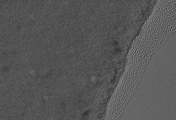
High resolution transmission electron microscopy (HRTEM) is a powerful tool for materials analysis. This technique provides visualization of the atomic lattice, providing important information about a materials structure, defects, homogeneity and its composition.
At CNS, we have four HRTEMs available for materials analysis. Each HRTEM is capable of high resolution imaging and diffraction analysis. A dedicated diffraction camera, HR-STEM mode, EDS and/or EELS detectors are available on some instruments. We have a selection of specialized specimen holders available for advanced TEM imaging and analysis.
More information on our JEOL ARM 200F TEM/STEM, JEOL 2010F TEM/STEM and JEOL 2100 TEM.
Focused Ion Beam
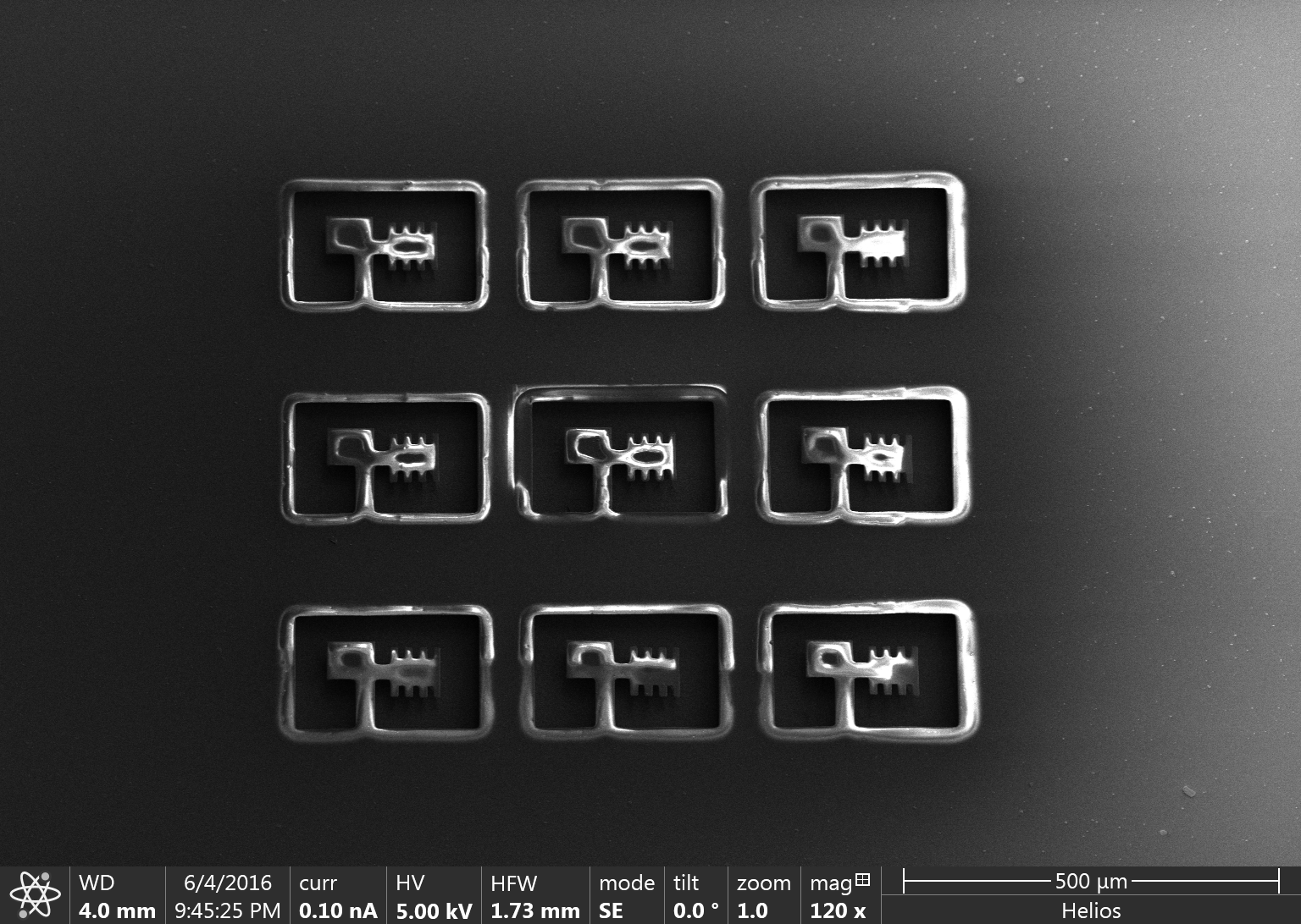
Focused Ion Beam systems use a finely focused beam of gallium ions to remove nanometers of material or deposit metals and insulators using gaseous precursors. These tools were originally developed for the semiconductor industry but have been readily implemented in the biological sciences, material sciences, applied physics, and geology fields.
At the CNS, we offer two dual beam FIB-SEM systems. These instruments have advanced milling, deposition, imaging and analytical capabilities. Our FIBs are particularly adept at preparing thin TEM specimens, high precision atom probe tips, and performing three dimensional imaging/analysis via automated successive milling.
More information on our Thermo Fisher Helios 660 FIB and our Zeiss Crossbeam FIB.
Scanning Electron Microscopy
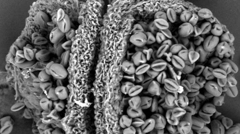
Scanning electron microscopy (SEM) is a versatile tool for studying surface topography from the nanoscale to macroscale. In addition, the local surface chemical composition and crystallography can be studies using SEM-based techniques such as energy dispersive x-ray spectroscopy (EDS), wavelength dispersive spectroscopy (WDS) and electron backscatter diffraction (EBSD).
At the Cambridge CNS location, we have two high resolution SEM systems, each with a different combination of detectors.
More information on our JEOL 7900 SEM and our Zeiss Ultra Plus SEM.
The Cambridge CNS laser laboratory enables its users to explore the behavior of complex systems using a wide array of optical and spectral imaging tools, ranging from high quality laser-scanning confocal imaging and Coherent Raman imaging instrumentation to conventional linear and nonlinear spectroscopies. These systems are capable of supporting a new type of optical microscopy: Stimulated Raman Scattering Microscopy for imaging based on intrinsic chemical vibrational signatures. Our systems are applicable to researchers working in diverse areas from traditional cell biology to cutting edge materials imaging and analysis.
Raman Spectroscopy
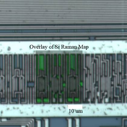
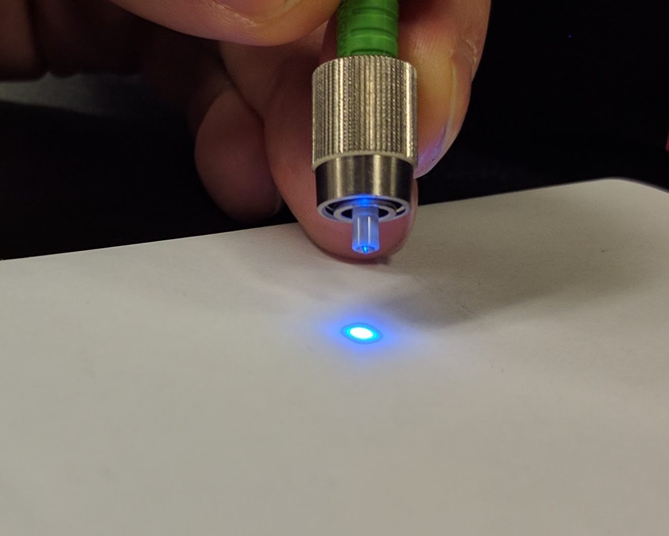
Raman spectroscopy facilitates the study of vibrational and other low frequency optical modes in a specimen. When combined with a motorized stage, such systems can be used to gain chemical information with sub-micron spatial resolution.
The Center for Nanoscale Systems provides a high resolution Raman system, Horiba LabRam Evolution system, which currently has 532nm and 633nm excitation laser lines. This has a 800mm spectrometer with 600 blaze grating and an 1800 blaze grating and a Synapse CCD detector. It has 10x, 20x LWD, 50x LWD, and 100X LWD microscope objectives. It is also equipped with a motorized confocal aperture, an XYZ motorized stage, duoscan mirrors, motorized polarization control, and SWIFT mapping options. An optical cryostat with electrical feed throughs is available for low temperature microPL spectroscopy.
More information on our Horiba Multiline Raman Spectrometer and Horiba Hyperspectral Darkfield Raman Spectrometer.
Fourier Transform Infrared Spectroscopy
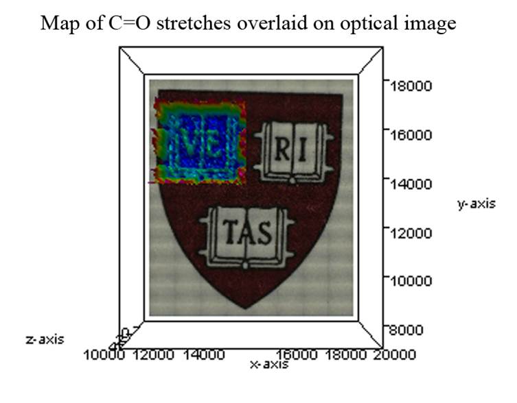
Fourier Transform Infrared Spectroscopy (FTIR) is a vibrational spectroscopy technique that provides molecular information about a sample. The FTIR systems can also be used to look for resonances in the 2-16 micron wavelength region from meta-materials.
CNS has two FTIR systems to accommodate different samples:
For microscopic samples or samples where the chemical mapping is desired, CNS has a Bruker Lumos FTIR microscope. The system has a liquid nitrogen cooled MCT detector and can collect signal in ATR, transmission, and specular reflection mode. It has a motorized stage and can perform chemical mapping of samples with ~10 um resolution.
For macroscopic samples or samples where an ensemble average measurement is needed CNS has a Perkin Elmer SpectrumOne with a single bounce germanium ATR crystal. Solids, powders, and liquids can all easily be analyzed with this system.
CNS has a variable angle specular reflection accessory for the Perkin Elmer system.
More information on our Thermo Fisher Nickolet FTIR spectrometer and Bruker Lumos FTIR.
Laser Systems
Advanced Laser systems form the backbone of any optics facility. CNS has several laser systems available for spectral analysis across a broad wavelength and temporal range. These include femtosecond lasers, scanning confocal systems and a white light laser with monochromator. Scanning confocal systems can be coupled to various microscopes, and we have the capability for two photon fluorescence imaging.
More information on our white light laser and Coherent Micro Femtosecond laser.
X-ray based analyses techniques enable detailed chemical composition studies of specimens. At the Center for Nanoscale Systems, our knowledgeable staff provide training and guidance on two advanced X-ray Photoelectron Spectroscopy (XPS) systems and an X-ray Fluorescence Spectrometer (XRF).
X-Ray Photoelectron Spectroscopy
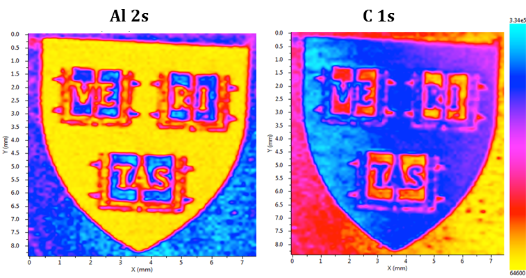
X-Ray Photoelectron Spectroscopy (XPS) is a widely used tool for material surface analysis. A monochromatic X-ray is used to probe the specimen surface to generate photoelectrons. Only photoelectrons from the top 10 nm of material surface are detected and analyzed, making this a highly surface-sensitive technique.
The XPS instruments at CNS can be operated in various data collection modes. XPS can be used to identify the elements present at the surface (qualitative analysis), and the concentration of elements at the surface (quantitative analysis). The chemical bonding state of elements (chemistry) can also be inferred from careful analysis of the data. Elemental mapping gives information on the distribution of elements across the surface, while depth profiling monitors changes in composition with depth into the surface.
More information on our Thermo Fisher Scientific K-Alpha+ and Nexsa XPS instruments.
X-ray Fluorescence
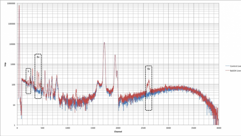
X-Ray Fluorescence (XRF) uses X-rays as a probe to generate emission process of characteristic X-rays from specimens. The measurement is non-destructive and provides reliable chemical composition of many types of materials in either solid or liquid form. Our XRF instrument can detect a wide range of elements, from sodium to uranium, with detection limits at the sub-ppm level.
More information on our Spectro XRF instrument.
Three dimensional tomographic analysis of specimens is a rapidly growing area, facilitating ultra-high resolution 3D renderings of materials specimens. The Center for Nanoscale Systems is at the forefront of these techniques, and our staff are specialists in sample preparation, data collection and analysis of data sets for a diverse range of challenging sample types. At CNS, we offer x-ray microtomography (micro-CT) and atom probe tomography (APT), along with specialized simulation packages and dedicated analysis workstations for data processing.
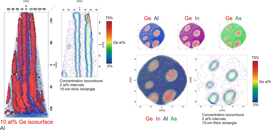
Atom Probe Tomography
Atom Probe Tomography (APT) systems provide atomic-scale imaging and chemical analysis. A very sharp tip is formed of the specimen and a high voltage is used to evaporate atoms from the tip apex (with the aid of laser or high voltage pulsing). Time-of-flight measurements with a position sensitive ion detector are used to determine the mass/charge ratio and extract the original position of each detected ion. This procedure is repeated until a 3-D map is constructed of the tip.
Our APT system can detect data sets of up to two billion atoms (approximately 1 cubic micron of material). It can detect any atom or isotope from the entire periodic table, and has a 37% detector efficiency. A 355nm ultrafast pulsed laser can be used for analyzing insulating/seminconducting specimens.
More information on our Cameca 3D Atom Probe.
X-ray Micro-CT
Micro-CT is an X-ray imaging technique capable of generating 3-D, cross-sectional and internal structure images. This technique uses micro-focused X-rays to create a non-destructive shadow image of an object based on X-ray absorption by the material. A computer is processes images from all directions and reconstructs the 3-D structure of the object from the intensity values in the projected shadow images. Multiple targets are available to accommodate a variety of specimen densities. Both the internal and surface structure can be observed with micro-meters resolution for biological samples, minerals, electronic components and material characterization.
Our micro-CT system can handle samples of up to 8inch by 8 inch in maximum cross-section. The system is equipped with X-ray guns either in reflection target mode (minimum 3 μm focal spot size) or transmission target mode. Four CT reconstruction computers are available for image processing.
More information on our X-Tek Micro-CT system and Zeiss Xradia Versa Micro-CT.
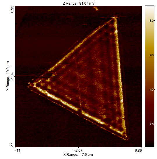
Our scanning probe facility provides a large selection of atomic force microscopy (AFM) and other advanced scanning probe microscopy (SPM) techniques. These instruments are used to study the two-dimensional surface structure of specimens from a diverse range of hard and soft materials.
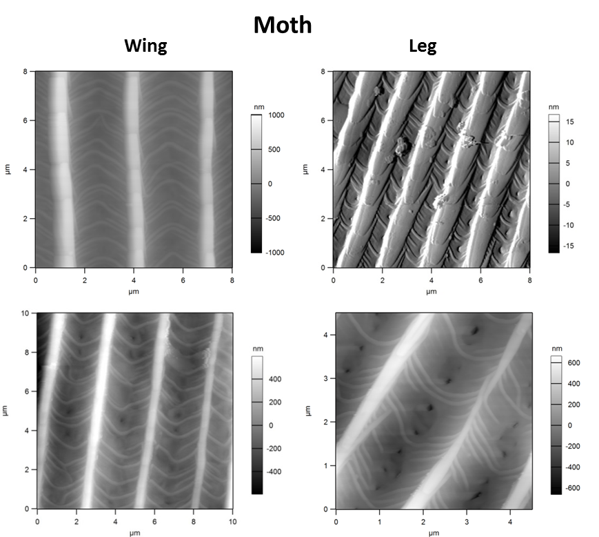
Atomic Force Microscopy
AFM is one of the most frequently used SPM techniques to study surface topography at the Center for Nanoscale Systems. In this technique, a sharp tip is used to probe the specimen surface in contact or tapping mode. This is used to produce a topographic and/or phase map showing spatial variations such as height and material contrast. AFM can be used to measure the force between the tip and specimen as a function of tip-sample distance. It can also be used for nano-lithography and nano-manipulation.
The scan-probe facility at CNS offers AFM with AC, Contact modes with 5 channels of imaging outputs, Nanolithography and Nanomanipulation, Conductive AFM (ORCA), MFM, EFM, Coax RF Scanning Probe Microscope. In addition, an array of advanced force measurements, controlled measurement environments (fluid, sample temperature, variable field) are supported. Also available is a combination of AFM and fluorescence optical microscope with high speed camera detection.
Optical nano-Imaging
Nowadays Atomic Force Microscopy is a general-purpose device used in many configurations for specific force characterization, including electric force microscopy, magnetic force microscopy, microwave impedance microscopy, multifrequency force microscopy, etc.
In its most recent applications AFM has also been proposed in different schemes for optical near-field imaging (SNOM) and spectroscopy at the nanoscale without detecting any light (PiFM).
At CNS, we are contributing to research on optical nano-Imaging with both optical near-field systems and photo-induced force detection.
More information on our Neaspec NSOM and Molecular Vista PFIM.