
Featured Research
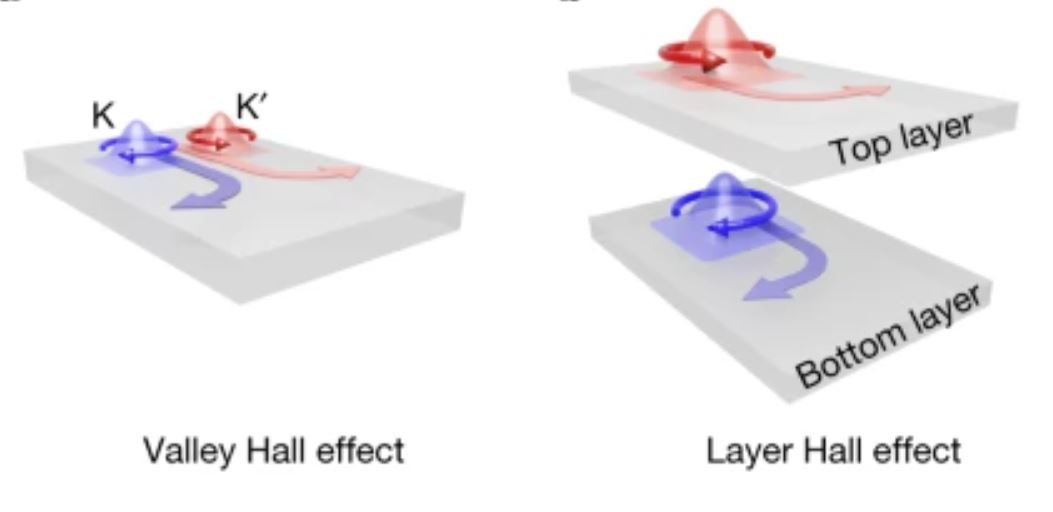
Su-Yan Xu’s group have discovered interesting topological modes in antiferromagnetic axion insulators. This Hall layer effect allows the researchers to better understand the Berry phase in these materials, which has novel spatial variation.
[+MORE]
Yacoby group demonstrates new quantum behavior at low magnetic fields in graphene
The Yacoby group has demonstrated an interesting quantum phenomena called Fractional Chern bands at low magnetic fields in magic angle twisted bilayer graphene. Full article can be found in Nature here or a summary of this work here.
[+MORE]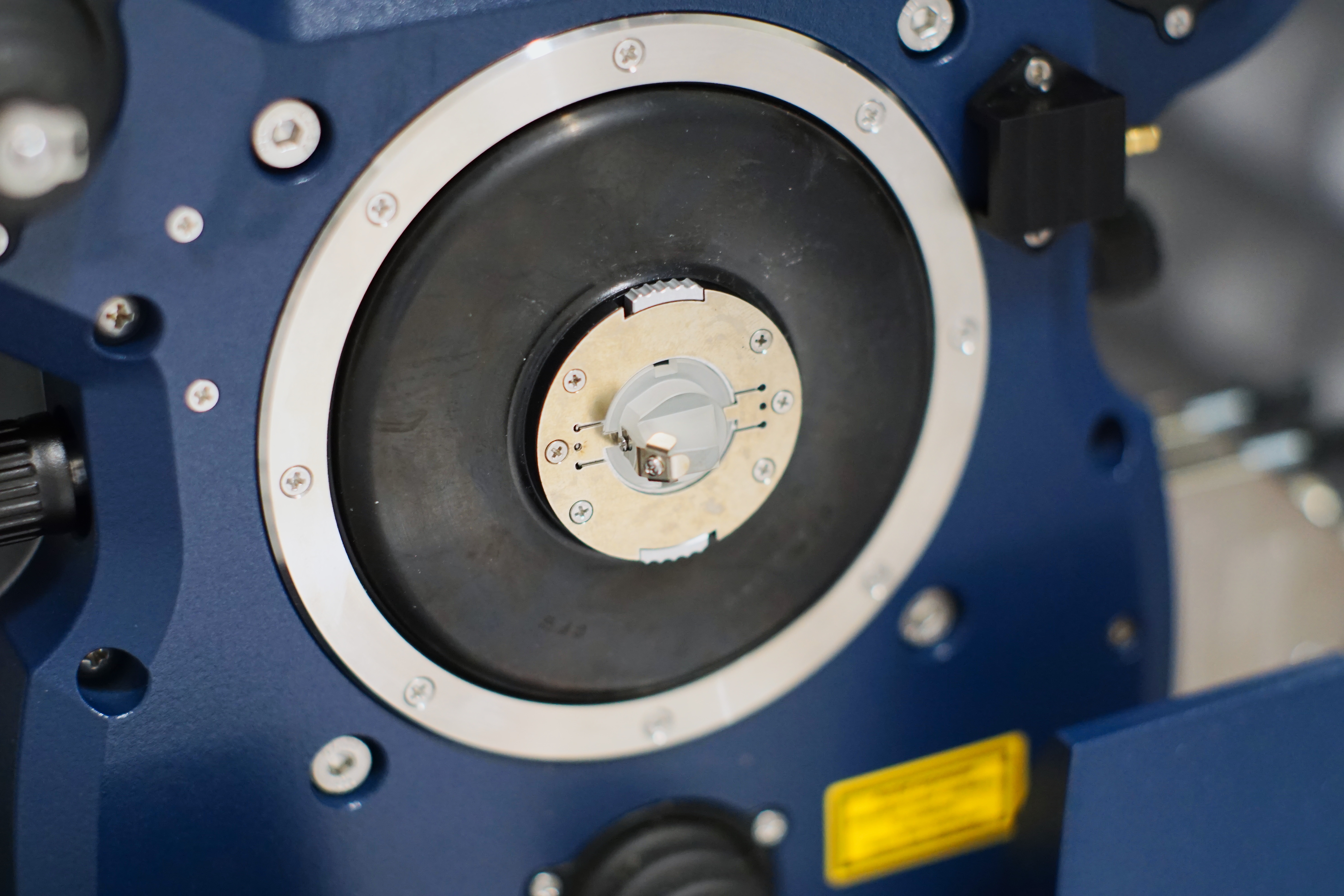
New CNS Facilities at the Allston SEC
The Center for Nanoscale Systems recently opened three new facilities in the Science and Engineering Complex (SEC) at Harvard University’s Allston Campus. Our new materials characterization lab houses a diverse selection of instrumentation for analyzing hard and soft materials, including thermal, mechanical, surface, particle, and chemical characterization. Our soft lithography facility is equipped for fabricating and replicating micrometer to nanoscale features using soft elastomeric materials, either through self-assembly or replica molding. Meanwhile, the new imaging lab has two high resolution electron microscopes, along with an array of electron microscopy sample preparation tools for hard and soft materials.
Click here for more information about the tools available in our Allston and Cambridge facilities of contact info@cns.fas.harvard.edu for more information.
[+MORE]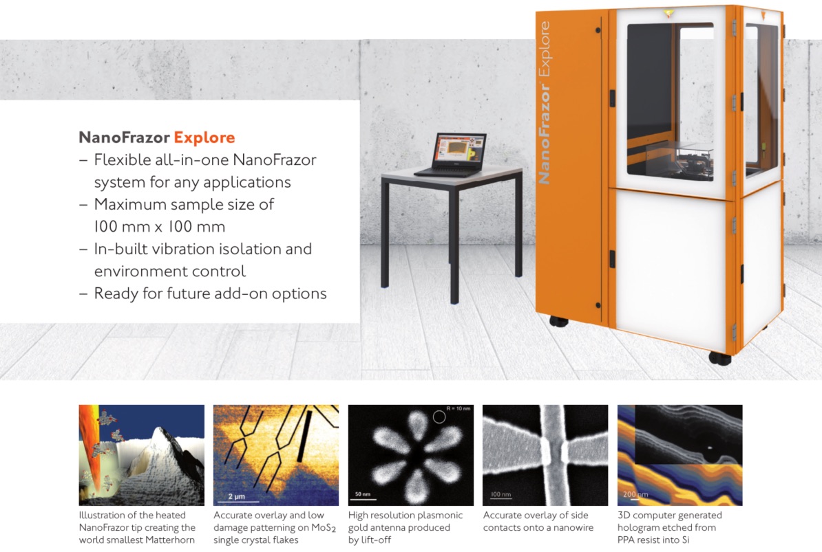
Hybrid Nanolithography System combining Thermal SPM and direct laser lithography in CNS
Thermal scanning probe lithography (tSPL) uses heated ultrasharp tips to write nanometer-scale structures by evaporating the resist. Commercialized by SwissLitho in 2014 under the name NanoFrazor, this technology has matured, and now enables researchers all over the world to avoid obstacles inherent to the conventional nanolithography tools. Many devices with novel geometries and unprecedented quality are produced using NanoFrazor, leading to interesting research results reported in many high impact publications.
The NanoFrazor is a versatile tool for micro- and nanotechnology thanks to the high resolution and markerless overlay capabilities without exposing the sample to charged particle beams like electrons or ions. The NanoFrazor Explore DLS combines thermal scanning probe lithography with direct laser sublimation (DLS) – an add-on to speed up the microlithography process patterning of larger features. SwissLitho teamed up with Heidelberg Instruments to develop the integrated laser and the optics. The Harvard’s Center for Nanoscale Systems (CNS) will be the first facility to receive such a new hybrid system. CNS already has a positive experience as a beta site for new products from Heidelberg Instruments. In 2015, the CNS has acquired the MLA150, which quickly became an important workhorse for almost all users. As a result of the successful collaboration between CNS and Heidelberg, the MLA150 has been installed in many research facilities and even in production settings, replacing conventional mask aligners and eliminating the need for masks at all.
What makes NanoFrazor Explorer DLS stand out, in addition to the range and precision of its operation, is in-situ imaging during the writing process and the Closed Loop Lithography approach. Thanks to that, 3-dimensional nanostructures can be implemented with single nanometer precision. Also, there is no need to use wet chemistry for resist development, or to tediously correct for proximity effects like in electron beam lithography. NanoFrazor does not require vacuum since no focussed electrons or ions are used. These characteristics make the NanoFrazor an excellent tool for nanolithography on sensitive materials, in particular, for quick and precise patterning of the sample electrodes or etch masks on nanowires or 2D materials. Besides standard resist based nanolithography the hot tip of the NanoFrazor can be used to locally heat up any surface at the nanoscale, hence triggering local chemical reactions or phase changes.
The first NanoFrazor Explore DLS will arrive at CNS in early April 2019. Harvard is one of the beta-testing sites for the new instrument, so CNS users get the chance to exploit the advanced features as early as possible. Beta testing of the NanoFrazor Explore DLS will kick off with a webinar for prospective users, introducing the fundamentals and the possibilities of the tool. The webinar will take place on March, 27th at 10 AM EST (https://global.gotomeeting.com/join/424882261) Attendees of the webinar can sign up for training at the tool. Researchers are invited to contact the SwissLitho team with inquiries at any time to get application-specific support directly from the developers of the technology.
After the installation, the NanoFrazor Explore DLS can be used by all CNS users and on-site trainings are offered. To further strengthen the knowledge of its tSPL technology and possibilities for cutting-edge device fabrication, we also will hold a seminar/workshop on May, 2nd (with Prof. Riedo* from NYU as a key speaker).
__________________________
*Zheng et al., Nature Electronics, 2,17–25 (2019)
| March, 27th (10AM EST): Webinar NanoFrazor demo
May, 2nd: Workshop/Seminar @CNS |
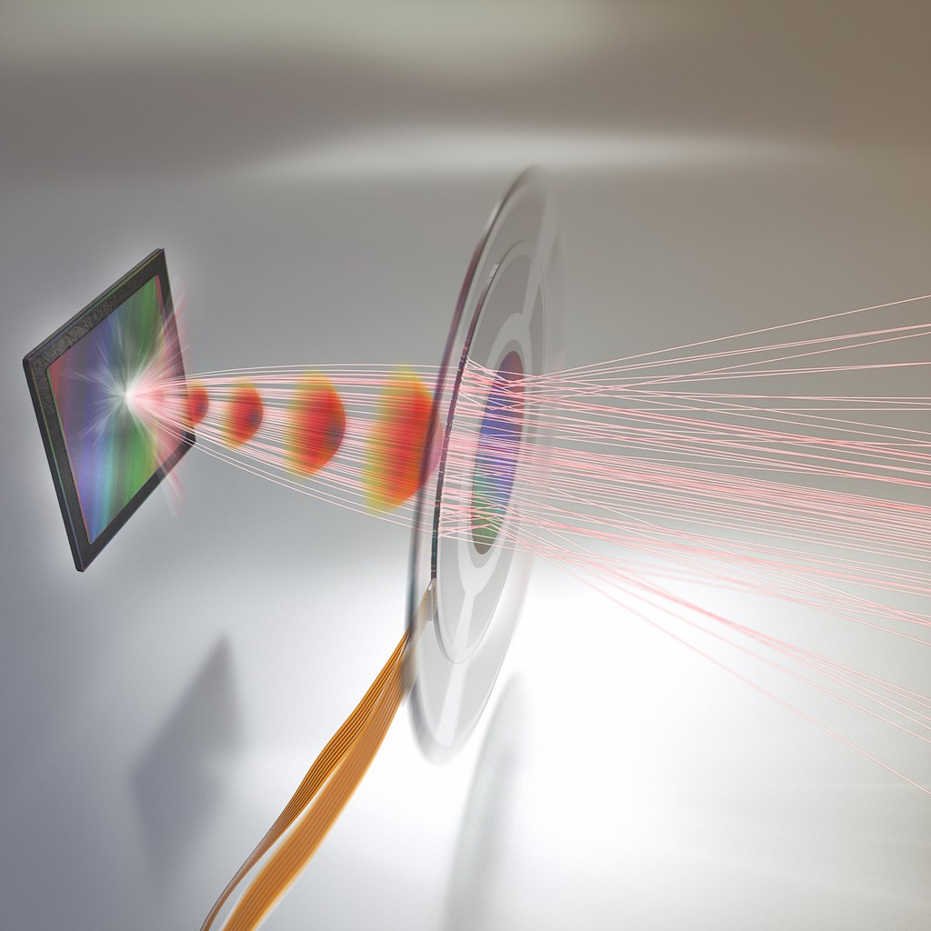
Researchers Combine Artificial Eye and Artificial Muscle
Inspired by the human eye, researchers at the Harvard John A. Paulson School of Engineering and Applied Sciences (SEAS) have developed an adaptive metalens that is essentially a flat, electronically controlled artificial eye. The adaptive metalens simultaneously controls for three of the major contributors to blurry images: focus, astigmatism, and image shift.
The research is published in Science Advances.
“This research combines breakthroughs in artificial muscle technology with metalens technology to create a tunable metalens that can change its focus in real time, just like the human eye,” said Alan She, an SEAS graduate student at the Graduate School of Arts and Sciences, and first author of the paper. “We go one step further to build the capability of dynamically correcting for aberrations such as astigmatism and image shift, which the human eye cannot naturally do.”
“This demonstrates the feasibility of embedded optical zoom and autofocus for a wide range of applications, including cell phone cameras, eyeglasses, and virtual and augmented reality hardware,” said Federico Capasso, the Robert L. Wallace Professor of Applied Physics and Vinton Hayes Senior Research Fellow in Electrical Engineering at SEAS and senior author of the paper. “It also shows the possibility of future optical microscopes, which operate fully electronically and can correct many aberrations simultaneously.”
The Harvard Office of Technology Development has protected the intellectual property relating to this project and is exploring commercialization opportunities.
To build the artificial eye, the researchers first needed to scale up the metalens.
Metalenses focus light and eliminate spherical aberrations through a dense pattern of nanostructures, each smaller than a wavelength of light. Earlier metalenses were about the size of a single piece of glitter.
“Because the nanostructures are so small, the density of information in each lens is incredibly high,” said She. “If you go from a 100 micron-size lens to a centimeter-size lens, you will have increased the information required to describe the lens by 10,000. Whenever we tried to scale up the lens, the file size of the design alone would balloon up to gigabytes or even terabytes.”
To solve this problem, the researchers developed a new algorithm to shrink the file size to make the metalens compatible with the technology currently used to fabricate integrated circuits. In a paper recently published in Optics Express, the researchers demonstrated the design and fabrication of metalenses of up to centimeters or more in diameter.
“This research provides the possibility of unifying two industries, semiconductor manufacturing and lens-making, whereby the same technology used to make computer chips will be used to make metasurface-based optical components, such as lenses,” said Capasso.
Discovery should lead the way to lighter, less-bulky cameras, telescopes, and cellphones, SEAS researchers say
Next, the researchers needed to adhere the large metalens to an artificial muscle without compromising its ability to focus light. In the human eye, the lens is surrounded by ciliary muscle, which stretches or compresses the lens, changing its shape to adjust its focal length. Capasso and his team collaborated with David Clarke, Extended Tarr Family Professor of Materials at SEAS and a pioneer in the field of engineering applications of dielectric elastomer actuators, also known as artificial muscles.
The researchers chose a thin, transparent dielectic elastomer with low loss — meaning light travels through the material with little scattering — to attach to the lens. To do so, they needed to develop a platform to transfer and adhere the lens to the soft surface.
“Elastomers are so different in almost every way from semiconductors that the challenge has been how to marry their attributes to create a novel multifunctional device and, especially, how to devise a manufacturing route,” said Clarke. “As someone who worked on one of the first scanning electron microscopes (SEMs) in the mid-1960s, it is exhilarating to be a part of creating an optical microscope with the capabilities of an SEM, such as real-time aberration control.”
The elastomer is controlled by applying voltage. As it stretches, the position of nanopillars on the surface of the lens shift. The metalens can be tuned by controlling both the position of the pillars in relation to their neighbors and the total displacement of the structures. The researchers also demonstrated that the lens can simultaneously focus, control aberrations caused by astigmatisms, and perform image shift.
Together, the lens and muscle are only 30 microns thick.
“All optical systems with multiple components — from cameras to microscopes and telescopes — have slight misalignments or mechanical stresses on their components, depending on the way they were built and their current environment, that will always cause small amounts of astigmatism and other aberrations, which could be corrected by an adaptive optical element,” said She. “Because the adaptive metalens is flat, you can correct those aberrations and integrate different optical capabilities onto a single plane of control.”
Next, the researchers aim to further improve the functionality of the lens and decrease the voltage required to control it.
To read the full story visit the Harvard Gazette website.
[+MORE]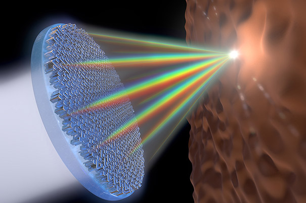
Single metalens focuses the entire visible spectrum of light to one point
Metalenses — flat surfaces that use nanostructures to focus light — have promised to revolutionize optics by replacing the bulky, curved lenses currently used in optical devices with a simple, flat surface, but previously metalenses had been limited in the spectrum of light they could focus well. Now a team of researchers at the Harvard John A. Paulson School of Engineering and Applied Sciences (SEAS) has developed the first single lens that can focus the entire visible spectrum — including white light — in the same spot and in high resolution, a feat previously achieved only by stacking multiple conventional lenses.
The research is published in Nature Nanotechnology.
Focusing the entire visible spectrum and white light — all the colors of the spectrum — is so challenging because each wavelength moves through materials at different speeds. Red wavelengths, for example, move through glass faster than the blue, so the two colors will reach the same location at different times, resulting in different foci. This creates image distortions known as chromatic aberrations.
Cameras and optical instruments use multiple curved lenses of different thicknesses and materials to correct these aberrations, which, of course, adds to a device’s bulk.
“Metalenses have advantages over traditional lenses,” said Federico Capasso, the Robert L. Wallace Professor of Applied Physics and Vinton Hayes Senior Research Fellow in Electrical Engineering at SEAS and senior author of the research. “Metalenses are thin, easy to fabricate, and cost effective. This breakthrough extends those advantages across the whole visible range of light. This is the next big step.”
Harvard’s Office of Technology Development (OTD) has protected the intellectual property relating to this project and is exploring commercialization opportunities.
The metalenses Capasso and his team developed use arrays of titanium dioxide nanofins to equally focus wavelengths of light and eliminate chromatic aberration. Previous research demonstrated that different wavelengths of light could be focused, but at different distances, by optimizing the shape, width, distance, and height of the nanofins. In this latest design, the researchers created units of paired nanofins that control the speed of different wavelengths of light simultaneously. The paired nanofins also control the refractive index on the meta-surface, and are tuned to result in different time delays for the light passing through different fins, ensuring that all wavelengths reach the focal spot at the same time.
“One of the biggest challenges in designing an achromatic broadband lens is making sure that the outgoing wavelengths from all the different points of the metalens arrive at the focal point at the same time,” said Wei-Ting Chen, a postdoctoral fellow at SEAS and first author of the paper. “By combining two nanofins into one element, we can tune the speed of light in the nanostructured material, to ensure that all wavelengths in the visible are focused in the same spot, using a single metalens. This dramatically reduces thickness and design complexity compared to composite standard achromatic lenses.”
“Using our achromatic lens, we are able to perform high-quality, white-light imaging. This brings us one step closer to the goal of incorporating them into common optical devices such as cameras,” said Alexander Zhu, co-author of the study.
Next, the researchers aim to scale up the lens, to about 1 cm in diameter. This would open a whole host of new possibilities, such as applications in virtual and augmented reality.
To read the full story visit the Harvard Gazette website.
[+MORE]
Curved lenses like those in cameras or telescopes are stacked to reduce distortions and clarify images. That’s why high-powered microscopes are so big and telephoto lenses so long. While lens technology has improved, it is still difficult to make a compact and thin lens.
But researchers from the Harvard John A. Paulson School of Engineering and Applied Sciences (SEAS) have demonstrated the first flat — or planar — lens that works highly efficiently within the visible spectrum of light, covering the whole range of colors from red to blue.
The lens can resolve nanoscale features separated by distances smaller than the wavelength of light. It uses an ultrathin array of tiny waveguides, known as a metasurface, which bends light as it passes through. The research is described in the journal Science.
“This technology is potentially revolutionary because it works in the visible spectrum, which means it has the capacity to replace lenses in all kinds of devices, from microscopes to cameras to displays and cell phones,” said Federico Capasso, Robert L. Wallace Professor of Applied Physics and Vinton Hayes Senior Research Fellow in Electrical Engineering, the senior author of the paper. “In the near future, meta-lenses will be manufactured on a large scale at a small fraction of the cost of conventional lenses, using the foundries that mass-produce microprocessors and memory chips.”
“Correcting for chromatic spread over the visible spectrum in an efficient way, with a single flat optical element, was until now out of reach,” said Bernard Kress, partner optical architect at Microsoft, who was not part of the research. “The Capasso Group’s meta-lens developments enable the integration of broadband imaging systems in a very compact form, allowing for next generations of optical sub-systems addressing effectively stringent weight, size, power, and cost issues, such as the ones required for high performance AR/VR [augmented reality/virtual reality] wearable displays.”
In order to focus red, blue, and green light — light in the visible spectrum — the team needed a material that wouldn’t absorb or scatter light, said Rob Devlin, a graduate student in the Capasso Lab and co-author of the paper.
Meta-Lenses at Visible Wavelengths
“We needed a material that would strongly confine light with a high refractive index,” he said. “And in order for this technology to be scalable, we needed a material already used in industry.”
The team used titanium dioxide, a material found in everything from paint to sunscreen, to create the nanoscale array of smooth and high-aspect ratio nanostructures that form the heart of the meta-lens.
“We wanted to design a single planar lens with a high numerical aperture, meaning it can focus light into a spot smaller than the wavelength,” said Mohammadreza Khorasaninejad, a postdoctoral fellow in the Capasso Lab and first author of the paper. “The more tightly you can focus light, the smaller your focal spot can be, which potentially enhances the resolution of the image.”
The team designed the array to resolve a structure smaller than a wavelength of light, around 400 nanometers across. At these scales, the meta-lens could provide better focus than a state-of-the art commercial lens.
“Normal lenses have to be precisely polished by hand,” said co-author Wei Ting Chen, a postdoctoral fellow in the Capasso Lab. “Any kind of deviation in the curvature, any error during assembling makes the performance of the lens go way down. Our lens can be produced in a single step — one layer of lithography and you have a high-performance lens, with everything where you need it to be.”
“The amazing field of meta-materials brought up lots of new ideas, but few real-life applications have come so far,” said Vladimir M. Shalaev, professor of electrical and computer engineering at Purdue University, who was not involved in the research. “The Capasso Group with their technology-driven approach is making a difference in that regard. This new breakthrough solves one of the most basic and important challenges, making a visible-range meta-lens that satisfies the demands for high numerical aperture and high efficiency simultaneously, which is normally hard to achieve.”
One of the most exciting potential applications, said Khorasaninejad, is in wearable optics such as virtual reality and augmented reality.
“Any good imaging system right now is heavy because the thick lenses have to be stacked on top of each other. No one wants to wear a heavy helmet for a couple of hours,” he said. “This technique reduces weight and volume and shrinks lenses thinner than a sheet of paper. Imagine the possibilities for wearable optics, flexible contact lenses, or telescopes in space.”
The authors have filed patents and are actively pursuing commercial opportunities.
[+MORE]
Advance in high-pressure physics
Nearly a century after it was theorized, Harvard scientists report they have succeeded in creating the rarest material on the planet, which could eventually develop into one of its most valuable.
Thomas D. Cabot Professor of the Natural Sciences Isaac Silvera and postdoctoral fellow Ranga Dias have long sought the material, called atomic metallic hydrogen. In addition to helping scientists answer some fundamental questions about the nature of matter, the material is theorized to have a wide range of applications, including as a room-temperature superconductor. Their research is described in a paper published today in Science.
“This is the Holy Grail of high-pressure physics,” Silvera said of the quest to find the material. “It’s the first-ever sample of metallic hydrogen on Earth, so when you’re looking at it, you’re looking at something that’s never existed before.”
In their experiments, Silvera and Dias squeezed a tiny hydrogen sample at 495 gigapascal (GPa), or more than 71.7 million pounds per square inch, which is greater than the pressure at the center of the Earth. At such extreme pressures, Silvera explained, solid molecular hydrogen, which consists of molecules on the lattice sites of the solid, breaks down, and the tightly bound molecules dissociate to transforms into atomic hydrogen, which is a metal.
While the work creates an important window into understanding the general properties of hydrogen, it also offers tantalizing hints at potentially revolutionary new materials.
“One prediction that’s very important is metallic hydrogen is predicted to be meta-stable,” Silvera said. “That means if you take the pressure off, it will stay metallic, similar to the way diamonds form from graphite under intense heat and pressure, but remain diamonds when that pressure and heat are removed.”
Understanding whether the material is stable is important, Silvera said, because predictions suggest metallic hydrogen could act as a superconductor at room temperatures.
“As much as 15 percent of energy is lost to dissipation during transmission,” he said, “so if you could make wires from this material and use them in the electrical grid, it could change that story.”
A room temperature superconductor, Dias said, could change our transportation system, making magnetic levitation of high-speed trains possible, as well as making electric cars more efficient and improving the performance of many electronic devices. The material could also provide major improvements in energy production and storage. Because superconductors have zero resistance, superconducting coils could be used to store excess energy, which could then be used whenever it is needed.
Metallic hydrogen could also play a key role in helping humans explore the far reaches of space, as a more powerful rocket propellant.

“It takes a tremendous amount of energy to make metallic hydrogen,” Silvera explained. “And if you convert it back to molecular hydrogen, all that energy is released, so that would make it the most powerful rocket propellant known to man, and could revolutionize rocketry.”
The most powerful fuels in use today are characterized by a “specific impulse” (a measure, in seconds, of how fast a propellant is fired from the back of a rocket) of 450 seconds. The specific impulse for metallic hydrogen, by comparison, is theorized to be 1,700 seconds.
“That would easily allow you to explore the outer planets,” Silvera said. “We would be able to put rockets into orbit with only one stage, versus two, and could send up larger payloads, so it could be very important.”
In their experiments, Silvera and Dias turned to one of the hardest materials on Earth, diamond. But rather than natural diamond, Silvera and Dias used two small pieces of carefully polished synthetic diamond and treated them to make them even tougher. Then they mounted them opposite each other in a device known as a diamond anvil cell.
“Diamonds are polished with diamond powder, and that can gouge out carbon from the surface,” Silvera said. “When we looked at the diamond using atomic force microscopy, we found defects, which could cause it to weaken and break.”
The solution, he said, was to use a reactive ion etching process to shave a tiny layer — just five microns thick, or about a tenth the thickness of a human hair — from the diamond’s surface. The diamond was then coated with a thin layer of alumina to prevent the hydrogen from diffusing into the crystal structure and embrittling it.
After more than four decades of work on metallic hydrogen, and nearly a century after it was first theorized, it was thrilling to see the results, Silvera said.
“It was really exciting,” he said. “Ranga was running the experiment, and we thought we might get there, but when he called me and said, ‘The sample is shining,’ I went running down there, and it was metallic hydrogen.”
“I immediately said we have to make the measurements to confirm it, so we rearranged the lab … and that’s what we did.”
[+MORE]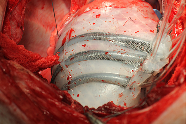
Soft robot helps the heart beat
Harvard University and Boston Children’s Hospital researchers have developed a customizable soft robot that fits around the heart and helps it beat, potentially opening new treatment options for people suffering from heart failure.
The soft robotic sleeve twists and compresses in synch with a beating heart, augmenting cardiovascular functions weakened by heart failure. Unlike currently available devices that assist heart function, Harvard’s soft robotic sleeve does not directly contact blood. This reduces the risk of clotting and eliminates the need for a patient to take potentially dangerous blood thinner medications. The device may one day be able to bridge a patient to transplant or help in cardiac rehabilitation and recovery.
“This research demonstrates that the growing field of soft robotics can be applied to clinical needs and potentially reduce the burden of heart disease and improve the quality of life for patients,” said Ellen T. Roche, the paper’s first author and a former Ph.D. student at the Harvard John A. Paulson School of Engineering and Applied Sciences (SEAS) and Wyss Institute of Biologically Inspired Engineering. Roche is currently a postdoctoral fellow at the National University of Ireland.
The research, published in Science Translational Medicine, was a collaboration between SEAS, the Wyss Institute, and Boston Children’s Hospital.
“This work represents an exciting proof-of-concept result for this soft robot, demonstrating that it can safely interact with soft tissue and lead to improvements in cardiac function. We envision many other future applications where such devices can delivery mechanotherapy both inside and outside of the body,” said Conor Walsh, senior author of the paper, John L. Loeb Associate Professor of Engineering and Applied Sciences at SEAS, and core faculty member at the Wyss Institute.
Heart failure affects 41 million people worldwide. Today, some of the treatment options are mechanical pumps called ventricular assist devices (VADs), which pump blood from the ventricles into the aorta, and heart transplants. While VADs are continuously improving, patients are still at high risk for blood clots and stroke.
To create an entirely new device that doesn’t come into contact with blood, Harvard researchers took inspiration from the heart itself. The thin silicone sleeve uses soft pneumatic actuators placed around the heart to mimic the outer muscle layers of the mammalian heart. The actuators twist and compress the sleeve in a motion similar to the beating heart.
The device is tethered to an external pump, which uses air to power the soft actuators.
The sleeve can be customized for each patient, said Roche. If a patient has more weakness on the left side of the heart, for example, the actuators can be tuned to give more assistance there. The pressure of the actuators can also increase or decrease over time, as the patient’s condition evolves.
The sleeve is attached to the heart using a combination of a suction device, sutures, and a gel interface to help with friction between the device and the heart.
The SEAS and Wyss engineers worked with surgeons at Boston Children’s Hospital to develop the device and determine the best ways to implant and test it on animal models.
“The cardiac field had turned away from idea of developing heart compression instead of blood-pumping VADs due to technological limitations, but now with advancements in soft robotics it’s time to turn back,” said Frank Pigula, a cardiothoracic surgeon and co-corresponding author on the study, who was formerly clinical director of pediatric cardiac surgery at Boston Children’s Hospital and is now a faculty member at the University of Louisville and division chief of pediatric cardiac surgery at Norton Children’s Hospital. “Most people with heart failure do still have some function left; one day the robotic sleeve may help their heart work well enough that their quality of life can be restored.”
More research needs to be done before the sleeve can be implanted in humans, but the research is an important first step toward an implantable soft robot that can augment organ function.
Harvard’s Office of Technology Development has filed a patent application and is actively pursuing commercialization opportunities.
“This research is really significant at the moment because more and more people are surviving heart attacks and ending up with heart failure,” said Roche. “Soft robotic devices are ideally suited to interact with soft tissue and give assistance that can help with augmentation of function, and potentially even healing and recovery.”
The research was co-authored by Markus A. Horvath, Isaac Wamala, Ali Alazmani, Sang-Eun Song, William Whyte, Zurab Machaidze, Christopher J. Payne, James Weaver, Gregory Fishbein, Joseph Kuebler, Nikolay V.Vasilyev, and David J. Mooney.
It was supported by a Translational Research Program grant from Boston Children’s Hospital, a Director’s Challenge Cross-Platform grant from the Wyss Institute for Biologically Inspired Engineering, Harvard School of Engineering and Applied Sciences, and the Science Foundation Ireland.
[+MORE]