Hybrid Nanolithography System combining Thermal SPM and direct laser lithography in CNS
June 2, 2026
Thermal scanning probe lithography (tSPL) uses heated ultrasharp tips to write nanometer-scale structures by evaporating the resist. Commercialized by SwissLitho in 2014 under the name NanoFrazor, this technology has matured, and now enables researchers all over the world to avoid obstacles inherent to the conventional nanolithography tools. Many devices with novel geometries and unprecedented quality are produced using NanoFrazor, leading to interesting research results reported in many high impact publications.
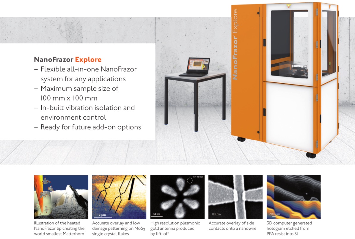
The NanoFrazor is a versatile tool for micro- and nanotechnology thanks to the high resolution and markerless overlay capabilities without exposing the sample to charged particle beams like electrons or ions. The NanoFrazor Explore DLS combines thermal scanning probe lithography with direct laser sublimation (DLS) – an add-on to speed up the microlithography process patterning of larger features. SwissLitho teamed up with Heidelberg Instruments to develop the integrated laser and the optics. The Harvard’s Center for Nanoscale Systems (CNS) will be the first facility to receive such a new hybrid system. CNS already has a positive experience as a beta site for new products from Heidelberg Instruments. In 2015, the CNS has acquired the MLA150, which quickly became an important workhorse for almost all users. As a result of the successful collaboration between CNS and Heidelberg, the MLA150 has been installed in many research facilities and even in production settings, replacing conventional mask aligners and eliminating the need for masks at all.
What makes NanoFrazor Explorer DLS stand out, in addition to the range and precision of its operation, is in-situ imaging during the writing process and the Closed Loop Lithography approach. Thanks to that, 3-dimensional nanostructures can be implemented with single nanometer precision. Also, there is no need to use wet chemistry for resist development, or to tediously correct for proximity effects like in electron beam lithography. NanoFrazor does not require vacuum since no focussed electrons or ions are used. These characteristics make the NanoFrazor an excellent tool for nanolithography on sensitive materials, in particular, for quick and precise patterning of the sample electrodes or etch masks on nanowires or 2D materials. Besides standard resist based nanolithography the hot tip of the NanoFrazor can be used to locally heat up any surface at the nanoscale, hence triggering local chemical reactions or phase changes.
The first NanoFrazor Explore DLS will arrive at CNS in early April 2019. Harvard is one of the beta-testing sites for the new instrument, so CNS users get the chance to exploit the advanced features as early as possible. Beta testing of the NanoFrazor Explore DLS will kick off with a webinar for prospective users, introducing the fundamentals and the possibilities of the tool. The webinar will take place on March, 27th at 10 AM EST (https://global.gotomeeting.com/join/424882261) Attendees of the webinar can sign up for training at the tool. Researchers are invited to contact the SwissLitho team with inquiries at any time to get application-specific support directly from the developers of the technology.
After the installation, the NanoFrazor Explore DLS can be used by all CNS users and on-site trainings are offered. To further strengthen the knowledge of its tSPL technology and possibilities for cutting-edge device fabrication, we also will hold a seminar/workshop on May, 2nd (with Prof. Riedo* from NYU as a key speaker).
__________________________
*Zheng et al., Nature Electronics, 2,17–25 (2019)
| March, 27th (10AM EST): Webinar NanoFrazor demo
May, 2nd: Workshop/Seminar @CNS |