

Events
News
29 Jun, 2026
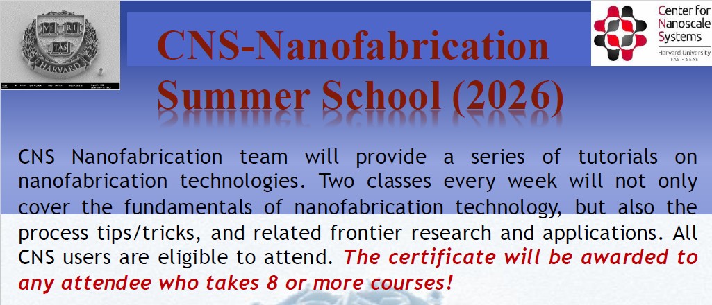
CNS Nanofabrication Summer School 2026
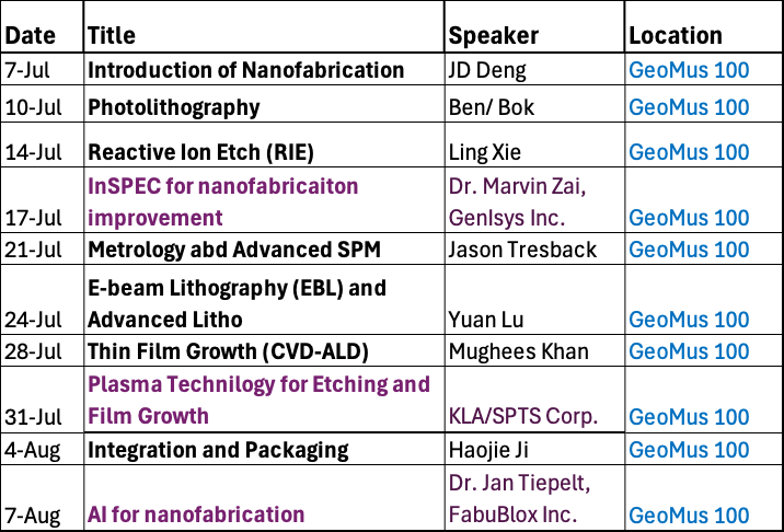
CNS Nanofabrication team will provide a series of tutorials on nanofabrication technologies. Two classes every week will not only cover the fundamentals of nanofabrication technology, but also the process tips/tricks, and related frontier research and applications. All CNS users are eligible to attend. The certificate will be awarded to any attendee who takes 8 or more courses!
Location: 100 Geo Lecture Hall, 24 Oxford St., Cambridge MA, 02138,
Time : Tuesday/Friday, 12:00-1:30pm,
Pizza lunch will be provided. The agenda may be changed according to the availability of staff and vendors.
Contact Ling Xie: lxie@cns.fas.harvard.edu; JD Deng: jdeng@cns.fas.harvard.edu
17 Feb, 2026
2026 CNS Spring Seminar Series
LISE 303, 1-2pm
Feb 20th: Prof. Donhee Ham, Harvard University
Feb 27th: Tony Song, Loncar Group, Harvard University
Mar 6th: David Kirkwood, Axelis
Mar 13th: Jonathan Zuberman, Kim Group, Harvard University
Mar 27th: Patrick Forrester, Yacoby Group, Harvard University
Apr 3rd: Ted Letsou, Capasso Group, Harvard University
Apr 10th: Erick Ramosmurillo, Alkemie
Apr 24th: Guanhao Huang, Loncar Group, Harvard University
May 1st: Jae Hyeong Lee, 3D-Architech
May 8th: Jason Yu, Hekstra Group, Harvard University
May 15th: Aaron Day, Loncar & Munday Groups, Harvard University
Contacts: Ling Xie lxie@cns.fas.Harvard.edu, William Wilson wwilson@cns.fas.Harvard.edu
[+MORE]Recent Publications
-
A silicon chip for water-based parallel DNA synthesis
Nature Electronics (2026). DOI: 10.1038/s41928-026-01664-7
-
Parallel enzymatic DNA synthesis using a semiconductor chip
Nature Electronics (2026). DOI: 10.1038/s41928-026-01662-9
-
Streamlined fabrication process of Si nanopillars for metasurface applications
J. Vac. Sci. Technol. B 1 January 2026; 44 (1): 012802. https://doi.org/10.1116/6.0005157
-
Bi surfactant-driven surface smoothing in InSb(100) epitaxy across extended growth temperatures
J. Vac. Sci. Technol. A 1 July 2026; 44 (4): 042705. https://doi.org/10.1116/6.0005473
-
Isotropic shrinkage of patterned vacancies enables three-dimensional nanoprecise metastructures for visible light applications
Nature Photonics https://doi.org/10.1038/s41566-026-01896-1
-
Topochemical oxidation of Ruddlesden–Popper nickelates reveals new structural family: oxygen-intercalated layered perovskites.
J. Am. Chem. Soc. 2026, 148, 6, 5873–5880.
-
Power Handling Modeling of Micro-and Nanoacoustic Resonators
0
-
High-Performance Solidly Mounted Bidimensional Mode Resonators (S2MRs) Operating Around 16 GHz
0
-
18 GHz Filters based on Cross-Sectional Lamé Mode Resonators (CLMRs)
1
-
Thin absorber AlInAsSb SACM APDs with photon-trapping gratings for eSWIR applications
Hannaneh Karimi, Qi Lin, Evan L. Simmons, Byron D. Aguilar, J. Andrew McArthur, Artem Talanov, Kubra Circir, A. Adam Dadey, Ellie Wang, Dekang Chen, Veronica Fisher, Tanner Pearson, Kyle J. Dorsey, Seth R. Bank, and Joe C. Campbell, "Thin absorber AlInAsSb SACM APDs with photon-trapping gratings for eSWIR applications," Optica 12, 1931-1935 (2025)
 WILLIAM WILSON
EXECUTIVE DIRECTOR
Directors Welcome
The Center for Nanoscale Systems (CNS) at Harvard University was created with a very clear vision: To provide a collaborative multi-disciplinary research environment to support of the creation and evolution of world-class nanoscience and technical expertise, for the Harvard research community as well as the larger community of external researchers both from academia and industry.
Our Core Values:
Facilitating leading-edge, multi-disciplinary, research a
[+MORE] ROBERT WESTERVELT
DIRECTOR